United States Photomask Market Size and Share 2025-2034
The United States Photomask Market is a key enabler of semiconductor fabrication, flat panel displays, MEMS, and nanotechnology devices. It is projected to grow at a CAGR of 3.00% between 2025 and 2034, fueled by rising semiconductor production, 5G, AI chips, and surging demand for high‑performance electronics.
United States Photomask Market Overview
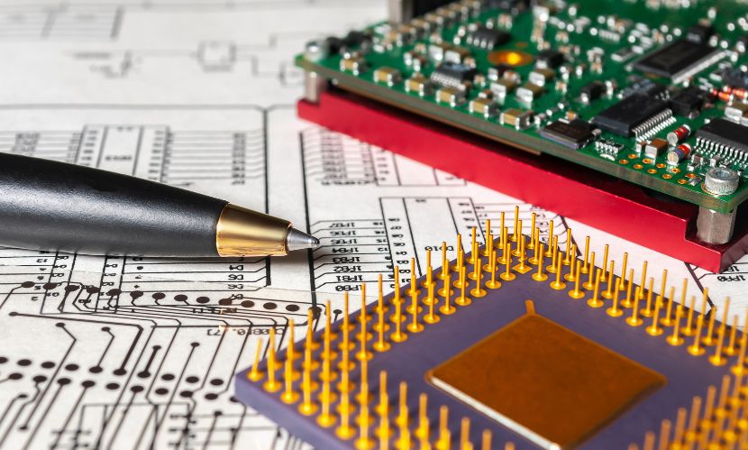
Photomasks are precision-patterned plates used in photolithography to transfer circuit designs onto silicon wafers or display substrates. As chip manufacturing nodes shrink and display resolutions increase, demand for advanced masking—such as phase shift masks and reticles—rises. The United States Photomask Market Growth is expanding accordingly, supported by investments in domestic foundries and R&D.
Segment: Type
Reticles
Used in advanced lithography for IC manufacturing—scalable exposures using step-and-repeat or stepper systems. Reticles are critical in high‑volume semiconductor fabs.
Standard Photomasks
Traditional chrome-on-glass masks used in legacy IC, MEMS, and less-demanding applications. They remain a stable component of the United States Photomask Market.
Phase Shift Masks (PSM)
Sophisticated masks that improve resolution by shifting phase of incident light. Essential in advanced IC nodes and lithography below 10nm. High precision and cost yield smaller but growing share of market.
Others
Includes binary masks for displays, embedded reticle sets, and specialty masks for R&D labs and nanotech applications. These niche types add breadth to mask‑shop services.
View the Complete Table of Contents in the Free Sample – Click Here
Segment: Application
Semiconductor and IC Manufacturing
The largest application segment: photomasks enable patterning of logic and memory chips. As U.S. foundries expand (e.g., Intel, TSMC), domestic mask demand rises, anchoring the United States Photomask Market.
Flat Panel Display Manufacturing
Photomasks are used to pattern pixels on LCD and OLED panels. Display fabs in California and international partnerships support mask procurement.
MEMS Devices
Micro-electro-mechanical systems—sensors, micro-actuators—use photomask patterning for micro-scale structures. These specialized devices feed both industrial and consumer electronics sectors.
Nanotechnology
Research and prototype fabrication for chips, materials, and biomedical sensors rely on ultra-precision photomasks—often custom or prototype reticles.
Others
Includes photovoltaic cell patterning, microfluidics, and advanced packaging masks—supplying labs and niche manufacturers.
Regional Insights in the U.S.
New England: R&D hubs and small foundries with niche photomask demand for MEMS and nanotech research.
Mideast: High semiconductor fabrication and fab expansion in areas like New York and Pennsylvania support mask procurement.
Great Lakes: Legacy manufacturing states (Michigan, Ohio) contribute demand for both standard and specialty masks in industrial electronics.
Plains: Limited photomask demand outside academic or agricultural research institutions.
Southeast: Growth in electronics assembly and foundry expansions in North Carolina and Georgia boosting mask order volumes.
Southwest: California’s Silicon Valley and Phoenix area home to many chipmakers and mask shops—hub of the United States Photomask Market.
Rocky Mountain: Smaller demand, though labs in Colorado and Utah use masks for prototyping.
Far West: California leads in display fabs, chip packaging, mask R&D, and state-of-the-art mask shops—key region for market growth.
Companies Covered
Key providers driving the United States Photomask Market:
Toppan Photomasks, Inc. – Major global mask supplier, with U.S. operations serving foundries and R&D.
DNP Photomask – Japanese parent, U.S. mask shop providing advanced reticles and phase-shift solutions.
Photronics, Inc. – One of the largest U.S.-based photomask fabricators, serving IC and display manufacturers.
Hoya Corporation – Offers mask fabrication and lens technology supporting semiconductor ecosystems.
Nippon Filcon Co., Ltd. – Specialty reticle provider with U.S. clients in both R&D and legacy IC.
Others – Small mask shops and academic spin-offs supporting MEMS and prototyping markets.
Key Trends & Growth Drivers
Onshoring of Semiconductor Manufacturing
Recent government investments (e.g., CHIPS Act) and capacity building in U.S. chip fabs boost domestic demand for photomasks.
Advanced Nodes Require Phase Shift Masks
As industry moves to 5nm and below, demand for phase shift masks grows sharply in advanced U.S. fabs.
OLED & High-Resolution Display Growth
Flat panel display fabs in partnership with U.S. firms demand high-precision masks for display pixel patterning.
MEMS and IoT Expansion
Rise of edge sensors and MEMS components in industrial and automotive markets fuels photomask demand for small-batch prototyping.
Nanotechnology Research and Startups
Labs at universities and startups often require custom photomasks—boosting niche sector growth within the United States Photomask Market.
Expansion of Mask Shops and Services
Domestic capacity expansion, lead-time reduction, and confidentiality requirements push manufacturers to rely on U.S. mask providers rather than overseas.
Mixed-Material and Hybrid Mask Fabrication
Development of hybrid photomasks combining nano features, embedded routing, and high-precision reticles for advanced packaging and logic chips.
Frequently Asked Questions (FAQs)
What is the projected growth of the United States photomask market?
The United States Photomask Market is estimated to grow at a CAGR of 3.00% from 2025 to 2034, driven by semiconductor and display production increases.
Which types of photomasks lead demand?
Reticles and phase shift masks are leading market segments, with standard masks taking up the rest; others serve niche applications.
What are the main applications for photomasks in the U.S.?
Key applications include semiconductor and IC manufacturing, flat panel display fabs, MEMS devices, and nanotechnology prototyping.
Which U.S. region dominates photomask use?
The Far West (California, Arizona) leads due to high concentration of chip fabs and mask shops; the Southeast also shows growing demand.
Who are the leading mask suppliers?
Major players include Photronics, Toppan Photomasks, DNP Photomask, Hoya, and Nippon Filcon, serving both fab and research communities.
How do phase shift masks differ from standard masks?
Phase shift masks enhance lithographic resolution using interference patterns—critical for sub-10nm nodes and advanced chip manufacturing.
Is MEMS driving any significant growth?
Yes, MEMS devices used in sensors and automotive applications are contributing niche but growing demand for custom, small-batch photomasks.
Will domestic mask capacity continue to expand?
Yes—mask shops in the U.S. are scaling up to support foundry localization, confidentiality protocols, and just-in-time supply to U.S. fabs.
The United States Photomask Market is set to widen—from a base of USD 1.99 billion to approximately USD 5.16 billion by 2034, growing at 3.00% annually. This growth is underpinned by expanding U.S. chip manufacturing, advanced node demands, and rising demand in display and MEMS sectors.
As mask technology evolves—from phase shift reticles to nanotechnology prototypes—domestic mask production capabilities become critical. Providers who invest in precision, speed, and confidentiality will be essential partners in the U.S. semiconductor ecosystem.
Media Contact:
Company Name: Claight Corporation
Email: sales@expertmarketresearch.com
Toll Free Number: +1-415-325-5166 | +44-702-402-5790
Address: 30 North Gould Street, Sheridan, WY 82801
Website: https://www.expertmarketresearch.com


Leave a Reply
Want to join the discussion?Feel free to contribute!